modem spi freq 4MHz |
||
|---|---|---|
| .. | ||
| h-files | ||
| .gitignore | ||
| .gitignore.bak | ||
| Makefile | ||
| README.md | ||
| complex_fifo.v | ||
| io.pcf | ||
| io_ctrl.v | ||
| lvds_rx.v | ||
| lvds_tx.v | ||
| output.txt | ||
| p1k | ||
| shell.nix | ||
| smi_ctrl.v | ||
| spi_if.v | ||
| spi_slave.v | ||
| sys_ctrl.v | ||
| top.asc | ||
| top.bin | ||
| top.blif | ||
| top.json | ||
| top.v | ||
| try-seeds.sh | ||
README.md
Overview
CaribouLite contains an FPGA device (ICE40 family) with 1280 LE. It has two designated roles:
- Step #1: Controlling and managing the RF front-end path, and other digital device control.
- Step #2: Streaming SMI I/Q data from the RPI to the modem, and from the modem LVDS back to the SMI interface.
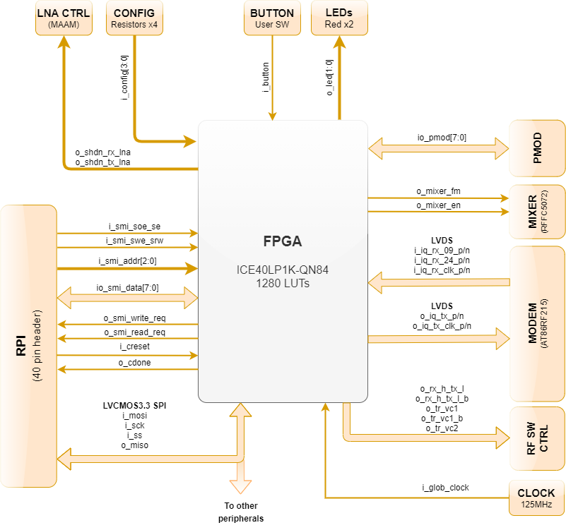
The above block diagram shows the FPGA's peripheral connections and their naming.
Convensions
- i_: input signal
- o_: output signal
- io_: input / output signal (controllable pin)
FPGA Internal Blocks
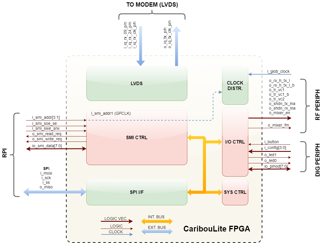 In the above diagram, the FPGA internal blocks of logic are shown. These blocks are segmented into Pink (Step #1) and Violet (Step #2).
Each subblock has a communal interface structure, module ID (within the system) and module version.
The subblocks are described below.
In the above diagram, the FPGA internal blocks of logic are shown. These blocks are segmented into Pink (Step #1) and Violet (Step #2).
Each subblock has a communal interface structure, module ID (within the system) and module version.
The subblocks are described below.
Generic Block Structure
This chapter describes the structure of a generic block within the FPGA internal blocks (SYS, IO, etc.). The minimal interfaces are shown below.
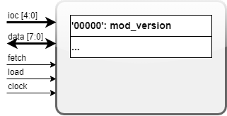
- All blocks shall respond to a default
'00000'opcode with their module-version. - The blocks have a 5-bit
IOCinterface carrying the internal opcode. - The input/output data have the width of 8-bits
- The generic module shall contain a clock input signal and will operate in a synchronous manner.
- The
fetchsignal shall "request" data (read operation) when it is asserted. - The
loadsignal shall "update" internal data (write operation) when it is asserted. - the
loadandfetchsignals shall not be asserted simultaneously.
SYS_CTRL - System Management Controller
This controller is in charge of communicating with the host, receiving instructions (over SPI), and delivering them to other subblocks. The SPI communication logic is integrated within this module and it is based on 2-byte transactions on each chip-select session - OPCODE => DATA. These short communication sessions are intended for simplicity and speed of operation. They ensure system state updates in <500 nsec (with 5Mbit/sec SCK). Even faster updates may be needed for several use-cases (e.g. fast frequency hopping), in which the SPI clock frequency will be increased (according to RPI documentation, SPI is functional up to ~10Mbit/sec reliably).
Opcode Structure
The Opcode is of 8-bit with the following structure:
| B7 | B6 | B5 | B4 | B3 | B2 | B1 | B0 |
|---|---|---|---|---|---|---|---|
| R/W | MID1 | MID0 | IOC4 | IOC3 | IOC2 | IOC1 | IOC0 |
R/W- a read / write indicator:'0': Read operation - fetching data IOC from the submodule MID'1': Write operation - loading data IOC to the submodule MID
MID[1:0]- Module ID as follows:'00': SYS_CTRL'01': IO_CTRL'10': SMI_CTRL'11': Reserved for future expansion
IOC[4:0]- Module Internal OpCode - these 5 bits will be further decoded by the submodule.
Note #1: IOC = '00000' is reserved for the READ-ONLY 'mod_version' property along with all modules thus it is not usable nor writable. This IOC shall not implicitly be described further in this document as it is the same for every module.
Note #2: The read-only (RO) properties shall not be writable and any attempt to write over them (i.e. R/W='1') will be ignored without any feedback to the host.
Note #3: IOCs that are not currently used by the modules shall be reserved for future expansions.
Internal OpCodes (IOCs)
IOC'00001': sys_version
Access Type: Read Only
Description: The version of the firmware currently running on the FPGA
Byte Structure:
| B7 | B6 | B5 | B4 | B3 | B2 | B1 | B0 |
|---|---|---|---|---|---|---|---|
| SV7 | SV6 | SV5 | SV4 | SV3 | SV2 | SV1 | SV0 |
IOC'00010': sys_manufacturer_id
Access Type: Read Only
Description: The firmware designer ID - along with the system version above gives a good identification of the system currently running. The sys_manufacturer_id of BabelBees shall be '00000001'.
Byte Structure:
| B7 | B6 | B5 | B4 | B3 | B2 | B1 | B0 |
|---|---|---|---|---|---|---|---|
| MI7 | MI6 | MI5 | MI4 | MI3 | MI2 | MI1 | MI0 |
IOC'00011': sys_error_status
Access Type: Read Only
Description: A report of errors ... TBD
Byte Structure:
| B7 | B6 | B5 | B4 | B3 | B2 | B1 | B0 |
|---|---|---|---|---|---|---|---|
| RES | RES | RES | RES | RES | RES | RES | ER0 |
ER0- write of RO (read only)
IO_CTRL - Pin-level I/O Controller
The IO_CTRL module is in charge of configuring and reading the Pin-IO resources of the FPGA. It spans over LED control, RF switching, power management, and more.
IOC'00001': data_io_ctrl_mode
Access Type: Read / Write
Description: The functional mode-of-operation of the system.
Byte Structure:
| B7 | B6 | B5 | B4 | B3 | B2 | B1 | B0 |
|---|---|---|---|---|---|---|---|
| RES | RES | RES | RFM2 | RFM1 | RFM0 | DBG1 | DBG0 |
DBG[1:0]- Debug mode operation'00': No-debug mode - the RFM field describes a set of pre-determines modes of operation'01': Debug mode - the RFM field directives are ignored and the RF-I/O settings are explicitly set in pin-level
RFM[2:0]- RF Mode of operation - this setting is active only when DBG='00''000': Low-power / inactive mode - all RF peripherals are turned off (LNAs, Mixer, etc.)'001': Bypass mode - the RF front-end wide-range tuning is turned off, and the modem 2.4GHz channel is operated within its native frequency range (2.4 - 2.483 GHz). The LNAs are switched off.'010': RX Lowpass mode - the RF frontend is set into RX mode (LNA active, PA deactivated) and is tuned to receive high-frequency signals (>2.483 GHz).'011': RX Highpass mode - the RF frontend is set into RX mode (LNA active, PA deactivated) and is tuned to receive low-frequency signals (<2.4 GHz).'100': TX Lowpass mode - the RF frontend is set into TX mode (LNA deactivated, PA active) and is tuned to transmit low-frequency signals (<2.4 GHz).'101': TX Highpass mode - the RF frontend is set into TX mode (LNA deactivated, PA active) and is tuned to transmit high-frequency signals (>2.4 GHz).'111': Reserved.
IOC'00010': data_io_ctrl_dig_pin
Access Type: Read / Write (bits [2:0])
Description: Digital pin control and read
Byte Structure:
| B7 | B6 | B5 | B4 | B3 | B2 | B1 | B0 |
|---|---|---|---|---|---|---|---|
| BTN | CFG3 | CFG2 | CFG1 | CFG0 | LDO28 | LED1 | LED0 |
BTN(ReadOnly): The current user push-button state (the 'USR' button on the PCB). While pushed,BTN='0', otherwise'1'.CFG[3:0](ReadOnly): The configuration resistors current state (R[41:38] respectively on the PCB). Assembled resistor shall show'0'value, otherwise'1'.LDO28: controlling the LDO (linear voltage regulator for RF) state -'1': on,'0': off.LED1: controlling the LED 'LD2' state on the PCB -'1': on,'0': off.LED0: controlling the LED 'LD1' state on the PCB -'1': on,'0': off.
IOC'00011': data_io_ctrl_pmod_pin_dir
Access Type: Read / Write
Description: PMOD connector bits IO pin direction
Byte Structure:
| B7 | B6 | B5 | B4 | B3 | B2 | B1 | B0 |
|---|---|---|---|---|---|---|---|
| PMODD7 | PMODD6 | PMODD5 | PMODD4 | PMODD3 | PMODD2 | PMODD1 | PMODD0 |
PMODD[7:0]: defined/reads out the pin direction of each of the 8 controllable bits in the PMOD connector. PMODD#='1': output, PMODD#='0': input.
IOC'00100': data_io_ctrl_pmod_pin_val
Access Type: Read / Write
Description: PMOD connector bits IO pin value
Byte Structure:
| B7 | B6 | B5 | B4 | B3 | B2 | B1 | B0 |
|---|---|---|---|---|---|---|---|
| PMOD7 | PMOD6 | PMOD5 | PMOD4 | PMOD3 | PMOD2 | PMOD1 | PMOD0 |
PMOD[7:0]: defined/reads out the pin value of each of the 8 controllable bits in the PMOD connector. PMOD#='1': set to logical '1', PMOD#='0': reset to logical '0'. If the direction of PMODD# of a specific pin is input, setting a'1'value will apply an internal weak pull up to that pin (TBD - Check).
IOC'00101': data_io_ctrl_rf_pin_state
Access Type: Read / Write
Description: Setting up / reading out the pin values controlling the RF front-end path switches.
Byte Structure:
| B7 | B6 | B5 | B4 | B3 | B2 | B1 | B0 |
|---|---|---|---|---|---|---|---|
| RXH | RXH_b | TRVC1 | TRVC1_b | TRVC2 | LNATX | LNARX | MXREN |
RXH- the value of theRX_H_TX_Lsignal in the PCB. This value is writeable and readable while the complement value at Bit#6 (RXH_b) is directly inferred from it (RXH_b=~RXH).TRVC1- the value of theTRVC1signal in the PCB. This value is writeable and readable while the complement value at Bit#4 (TRVC1_b) is directly inferred from it (TRVC1_b=~TRVC1).TRVC2- the value ofTRVC2signal in the PCB.LNATX- controlling the Transmit PA operation,'1': Shutdown,'0': Operational.LNARX- controlling the Receive LNA operation,'1': Shutdown,'0': Operational.MXREN- controlling the RF frequency mixer operation,'1': on,'0': off.
IOC'00110': data_io_ctrl_mixer_fm_prescale
TBD
IOC'00101': data_io_ctrl_mixer_fm_data
TBD
CLOCK_CTRL - Clocking Submodule Controller
TBD
SMI_CTRL - SerDes Contoller SMI <-> LVDS
TBD
License

This work is licensed under a Creative Commons Attribution 4.0 International License.