replace broken link |
||
|---|---|---|
| .. | ||
| __used_asset__ | ||
| logicdata | ||
| overlay | ||
| scans | ||
| schematic | ||
| README.md | ||
| README_DE.md | ||
README.md
RS41 Hardware
For general information about radiosondes Wikipedia.
For more information about the RS41 my website.
The blockwise structure of the RS41 is described in the following. The schematic in Eagle format, Logic Analyzer recordings of the functional blocks and high-resolution scans of the printed circuit boards are also provided.
The examination of the RPM411 daughter board with barometric sensor can be found in a seperate Repository and the OIF411 Ozone interface, as soon as available, in a separate subfolders.
Pull requests with improvements, translations and bug fixes are welcome!
ToDo
- identify unidentified components
- find unknown connections
- identify values of passive components
- find out which of the resistors entered in the schematic are in fact ESD-Surpressors etc..
- front end measurement in the climate chamber
- detailed description of the SPI bus
- detailed description of the UART between GPS and MCU
- functional investigation NFC interface
- sniffing of communication between RI41 Groundcheck Device and RS41
- receive and reverse flashdump of the controller
Introduction
The sonde is to be divided into six functional blocks, which are highlighted in the following picture.
Reverse engineering is complicated by the fact that the circuit board has four layers.
Powersupply
The power supply can be divided into three parts
- a boost converter generates 3.8 V from the variable battery voltage
- three Low Dropout Regulators (LDOs) each generate a 3 V rail for different blocks
- a hard-wired logic determines the operating state of the boost converter and thus of the sonde
Boost converter
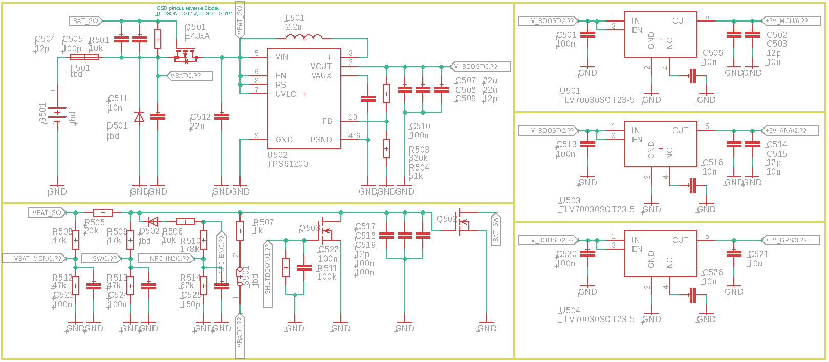
A TPS61200 U502 from TI is used for the boost converter, whose circuitry corresponds to the typical application. The input circuit contains an SMD fuse F501 and a clamping diode D501. Between battery and boost converter there is a P-channel MOSFET Q501, which is closed by the pull-up resistor R501 during storage. Q501 can be opened or closed by a hardwired logic (see below) to switch the sonde on or off.
LDOs
TVS70030 from TI are used. U501 generates the voltage for the microcontroller (MCU), U503 for the measurement frontend and U504 for the GPS module. Pin 4 of the LDOs, which is NC according to the data sheet, is decoupled against ground, probably so that pin compatible versions like the MAX8887 can be used.
Hard wired logic
The P-channel MOSFET Q501 discussed above is controlled by an N-channel MOSFET Q502.
- The sonde is on when this transistor is closed, which means its gate is HIGH.
- The sonde is off when this transistor is open, which means its gate is LOW.
Via R506 and D502 a one-way rectified signal from the NFC coil reaches the gate. This allows the probe to be switched on via NFC. Furthermore this signal is also used for communication with the RI41 Groundcheck Device and via the voltage divider R510 and R514/C525 brought to the MCU.
Once the sonde is switched on, it is kept in this state by the switched battery voltage, which is fed to the gate via R505.
To switch it off again, the MCU can close the N-channel MOSFET Q503, which brings the gate from Q502 to LOW.
The button at the bottom of the probe S501 switches the gate from Q502 via R507 to HIGH. The microcontroller can also query the status of the button, the gate voltage of Q502 is fed via the voltage dividers R506 and R512/C524 to an ADC input of the MCU for this purpose. The lower voltage drop via R507, which leads to a higher gate voltage when this is pressed, is evaluated here.
Finally, the battery voltage itself can also be evaluated by the MCU via the voltage dividers R508 and R512/C524.
Microcontroller
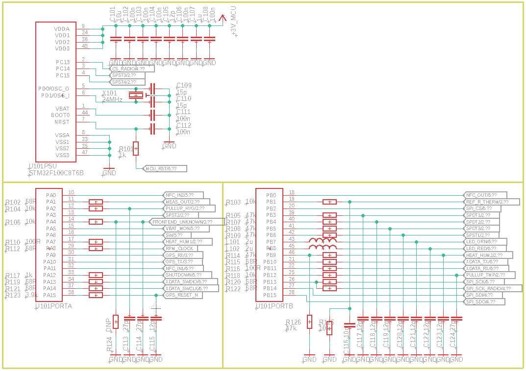
The microcontroller is a STM32F100C8 U101 from ST in LQFP48 package, which gets its clock from the 24 MHz crystal X101. Apart from the fact that all IO pins are used, it is only worth mentioning that RC low pass filters are present at many outputs.
Frontend
Circuit arrangement
Mechanically, the front end consists of the sensor boom, which is made of Flex PCB material covered with silver paint and connected to the board with a 20-pin FPC connector. The sensor boom includes a PT1000 temperature sensor, which is designed as a wire (the characteristic 'hook'), and a ceramic hybrid module to measure humidity. It combines three functions
- Measurement of air humidity using a capacitive hygrometer (dielectric constant of the hydrophilic dielectric changes and thus the capacitance of the capacitor over the measuring range.
- Measurement of the temperature of the module using a PT1000 as a feedback variable for controlling the module heating.
- Module heating via a thick film resistor. During flight, the module is kept 5 K above ambient to prevent condensation. During the preflight check it is heated to remove impurities and to perform a zero humidity check. There is no on-site calibration in the Ground Check Device for temperature.
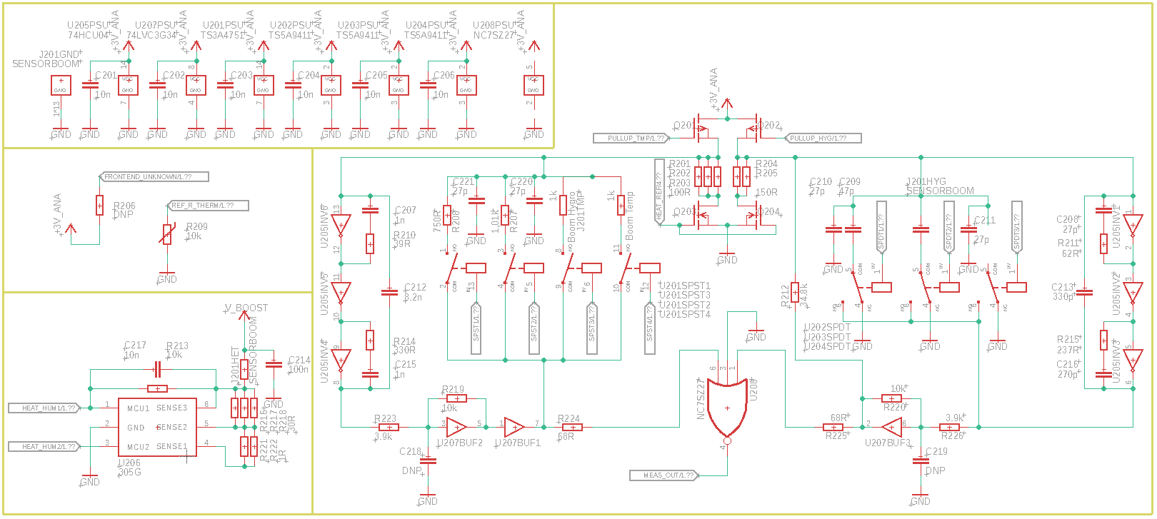
In addition, two reference resistors R208 and R209, one reference capacitor C209, five heating resistors R201-205 and the MOSFETs Q203-204, required to control these resistors, as well as an thermistor R209, are available on an area delimited by milled slots from the rest of the printed circuit board. No heating of the references could be observed in tests at room temperature.
Circuit topology
Electrically seen, the frontend consists of two ring oscillators for temperature and humidity, whose frequency is varied by variable impedances (e.g. the sensors) inserted into the feedback path with the help of analog switches.
Each ring oscillator is formed by 3/6 of a 74HCU04 Hex Inverter U205. Three inverters are connected in series. The first and third inverter are feedbacked directly via an RC series element C207/R210, R214/C215, C208/R211, R215/C216, the entire ring oscillator via a capacitor C212, C213. Both ring oscillators can be pulled to +3 V by a P-channel MOSFET Q201, Q202 at the first inverter with separate control, which corresponds to ground at the output, to deactivate them. The heating resistors for the reference, which can be activated by closing Q203, Q204 with closed P-channel MOSFETs Q201, Q202, are also located at the input of the inverters.
The feedback path for the temperature measurement consists of 2/3 buffers of a 74LVC3G34 U207 and two resistors R219 and R223, which probably are used for the fine tuning of the resonance frequency. This is followed by four single pole single throw (SPST) switches TS3A4751 U201, the NO of which is connected to the output of the buffer and which each switch one of the four possible measuring resistors (temperature/humidity/Ref1/Ref2) into the feedback path. The measuring tap is located between buffer and switch with a series resistor R224.
In the feedback path of the humidity measurement there is a circuit formed by the remaining buffer and two resistors R226 and R220. The measuring tap is made exactly like in the temperature measurement by a resistor R225. Furthermore in the feedback path there are three SPDT switches TS5A9411 U202-204, which switch the measuring and reference capacitor either into the feedback network or to ground. U205 has no connection between COM and the input of the first buffer, where there should normally be a reference capacitor, so this switch does not serve any obvious purpose. However, since it is driven in software like the other two, it can be assumed that the switches have an example-independent non-linear effect on the feedback frequency measured at this switch to compensate for it. Parallel to the switches, fixed feedback is applied via the resistor R212.
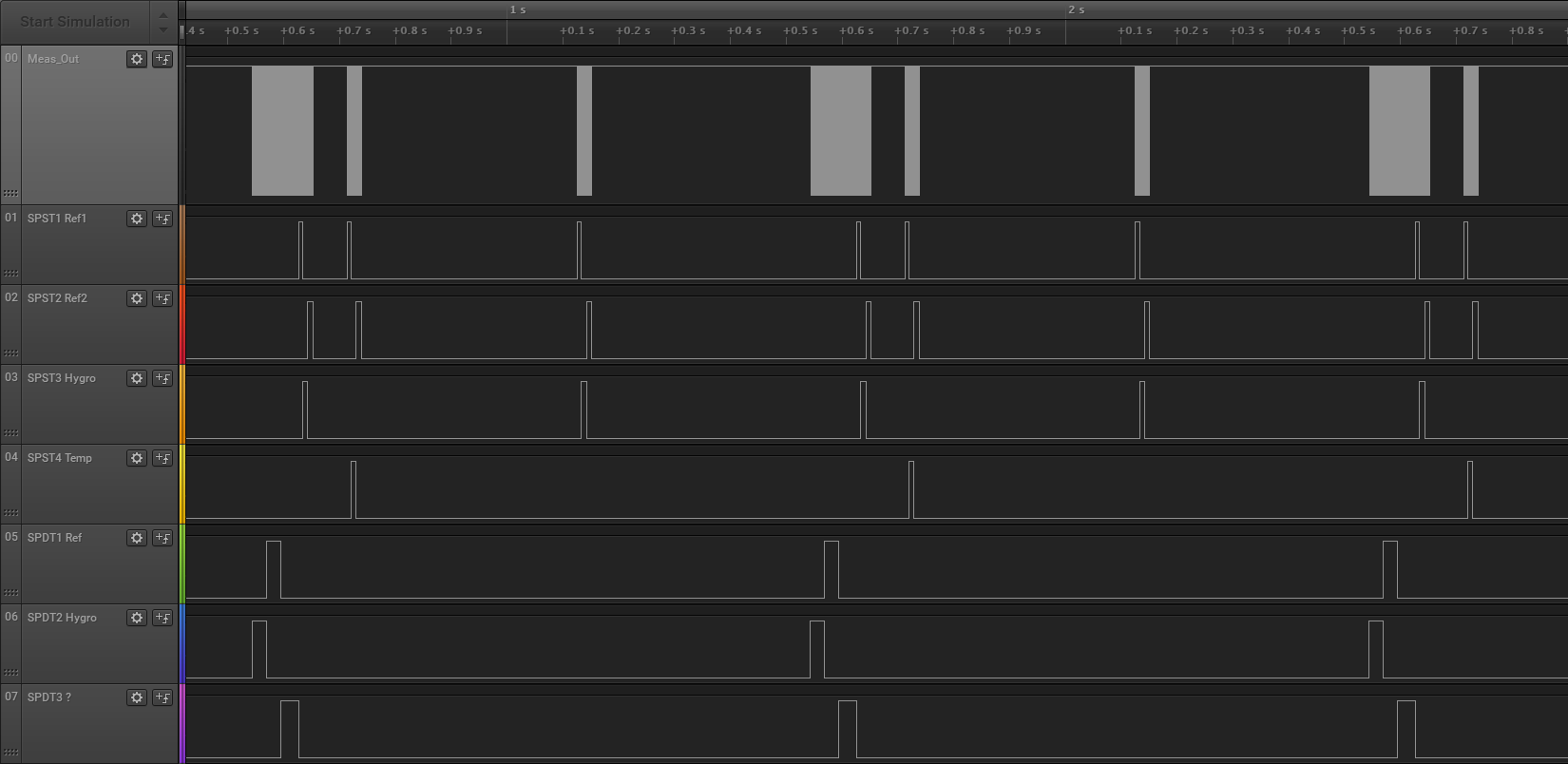
The two measurement outputs are converted in a NOR gate U208 and the result is sent to the MCU so that only one measurement can be performed at a time. Measurements with a Logic Analyzer show that the temperature is measured twice per second and the humidity once per second.
The heating of the humidity sensor is controlled by an unidentified component U206.
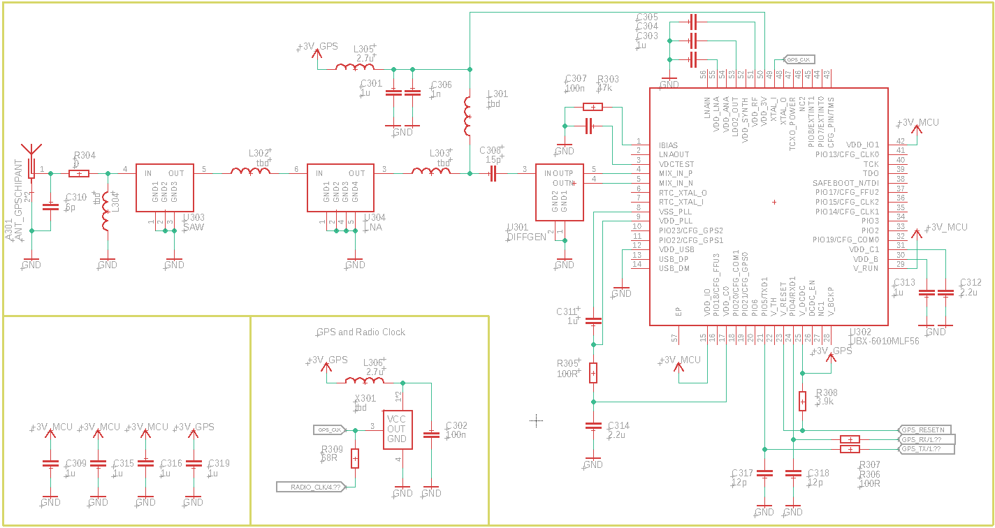
GPS
The GPS module UBX-6010 U302 is connected to the MCU via a UART. Apart from the discrete SAW filter and LNA, the circuitry corresponds essentially to the typical application.
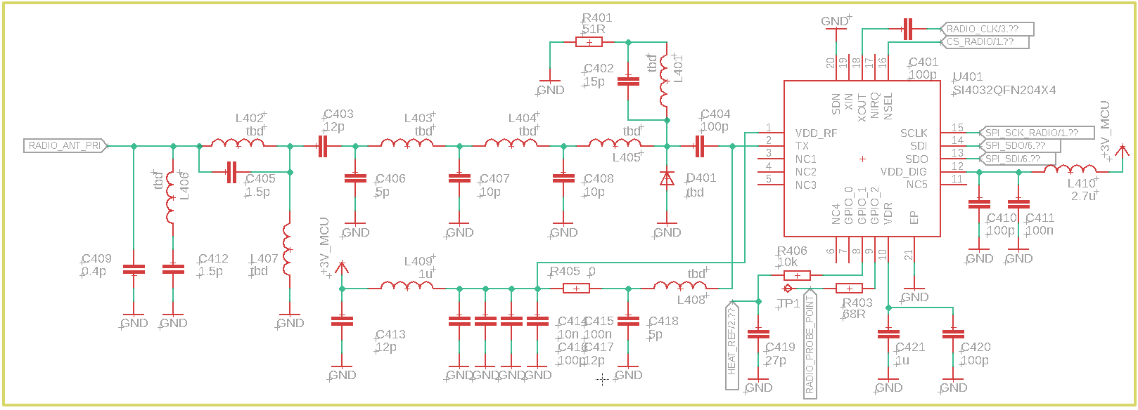
Radio
The radio interface is a one-chip solution with the Si4032 U401, which is connected to the MCU via SPI. Worth mentioning are the secondary, unused antenna pad and a track at TX, which purpose is currently unidentified.
The clock for the IC is provided from the oscillitator odf the GPS module, which is however only 26 MHz, it should be 30 MHz. This has to be taken into account when setting up radio frequencies.
GPIO1 switches the N-channel MOSFETS to heat the reference.
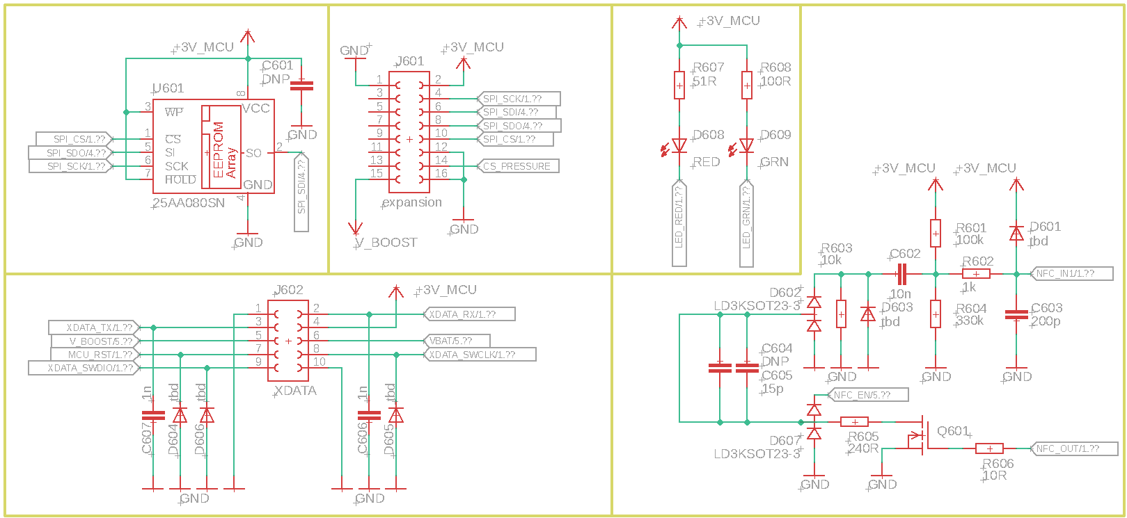
Interface
The following interfaces are provided
- EEPROM for the SGM version
- XDATA and programming connectors
- internal expansion connector
- NFC interface
EEPROM
On the back of the board there is a footprint for an SPI-EEPROM U601 with generic pinout, which shares the SPI bus with radio and internal expansion connector. This is most likely used to implement the Radio Silence Mode in the military version RS41-SGM, but so far no such sonde finding is known to confirm this hypothesis. In Radio Silence Mode, the sonde stores the ascent readings up to a certain altitude or time and sends them to the ground station alternating with the current frames. Since the internal memory of the MCU used, even in a configuration with more memory, is not sufficient for this purpose, the use of an EEPROM for this purpose seems to make sense.
XDATA and programming connectors
On the 2x5 2 mm pinheader J602 at the lower edge of the sonde the following connections are brought out
- XDATA as a UART; the pins can also be configured as I2C in violence of the XDATA standard
- SWD interface for flashing the MCU
- Reset pin of the MCU
- Battery voltage, 3.8 V boost voltage and 3 V MCU voltage
The mating ribbon connector is from the Amphenol Minitek series.
Pinout of XDATA connector                                    Pinout of connected ribbon cable
                 -------
           GND  | o   o |  XDATA_RX(PB11)                    > 1  GND
                |       |                                      2  XDATA_RX(PB11)
XDATA_TX(PB10)  | o   o |  +3V_MCU                             3  XDATA_TX(PB10)
               -        |                                      4  +3V_MCU
       V_Boost|   o   o |  VBAT                                5  V_Boost
               -        |                                      6  VBAT
       MCU_RST  | o   o |  SWCLK(PA14)                         7  MCU_RST
                |       |                                      8  SWCLK(PA14)
   SWDIO(PA13)  | o   o |  GND                                 9  SWDIO(PA13)
                 -------                                      10  GND
Internal expansion connector
The internal expansion connector J601 brings out the shared SPI bus an CS signal and a clock of unknown frequency, one of which is shared with the EEPROM, as well as the 3.8 V boost voltage and 3 V MCU voltage. There are unused pins which can be used e.g. for programming the mezzanine board.
The RPM411 barometric pressure module is the only mezzanine board in knowledge that uses this connection.
The type of connector is unknown and not trivial to find out. The specs are
- 2x8 poles
- 0.5 mm pitch
- 2 mm stacking height
- male and female connectors have locking pins that require holes in the footprint.
- The connector is mechanically loadable, there is no other mechanical connection between the two boards.
It would be desirable to find out the connector type for own developments. The "Tough Contact" P5KF connectors from Panasonic Electric Works could be compatible at a first glance.
NFC interface
The sonde can be switched on and parameterized via the NFC interface. The decoding takes place in the microcontroller, probably by bit banging, since there is no integrated NFC frontend available, which provides this wakeup functionality.
NFC is essentially based on two mechanisms for sending and receiving data
- When the Groundcheck Device sends data to the sonde, it pulses the 13.56 MHz carrier according to the data.
- When the probe sends data to the groundcheck device, it modulates the load it pulls from the transmission antennas field according to the data.
The received data is received differentially by the sonde. In parallel to the receiving coil there are two capacitors C604 and C605, then the two connections are clamped in a double diode D602/D607 against ground and one-way rectified. A connection is made to the voltage supply circuit described above.
The other connection is clamped again to ground with D603 and the one-way rectified signal is DC-coupled to ground with R603 and AC-coupled with C602. R601 and R604 bias this AC coupling before the signal is filtered by an RC low pass R602/C603 and clamped with D601 against the supply voltage of the MCU.
The modulation of the load resistor is carried out with the aid of a tap in front of the double diode to the voltage supply, by connecting the coil to ground via R605 and the N-channel MOSFET Q601. This allows a current path over R605, Q601 and R603 to be established for one half of the AC voltage signal.
Last but not least
Some project ideas, what to do with the gained knowledge
- Expand Amateur Radio firmware to include its own NFC interface and use of existing sensors
- alternative firmware for radiosonde use in the meteorological 400 MHz band
- Use as IoT room climate sensors in the 433 MHz ISM band
- Use as LoRaWAN nodes in the 433 MHz ISM band
- Development of our own mezzanine boards for space-saving extension boards
